Hongshi Tech Insights 07
Each article starts with a small question and explains one principle.
In the previous article, we looked at how electrons and holes recombine to produce light inside a MicroLED. This time, we turn to the edges of the light-emitting region. The sidewalls surrounding a pixel also affect how efficiently it emits light.
One important aspect of the MicroLED sidewall effect is nonradiative recombination caused by defects near the sidewalls. Some charge carriers are lost through this process without producing photons. Sidewall repair and surface passivation are ways to reduce these losses.
How sidewall defects form
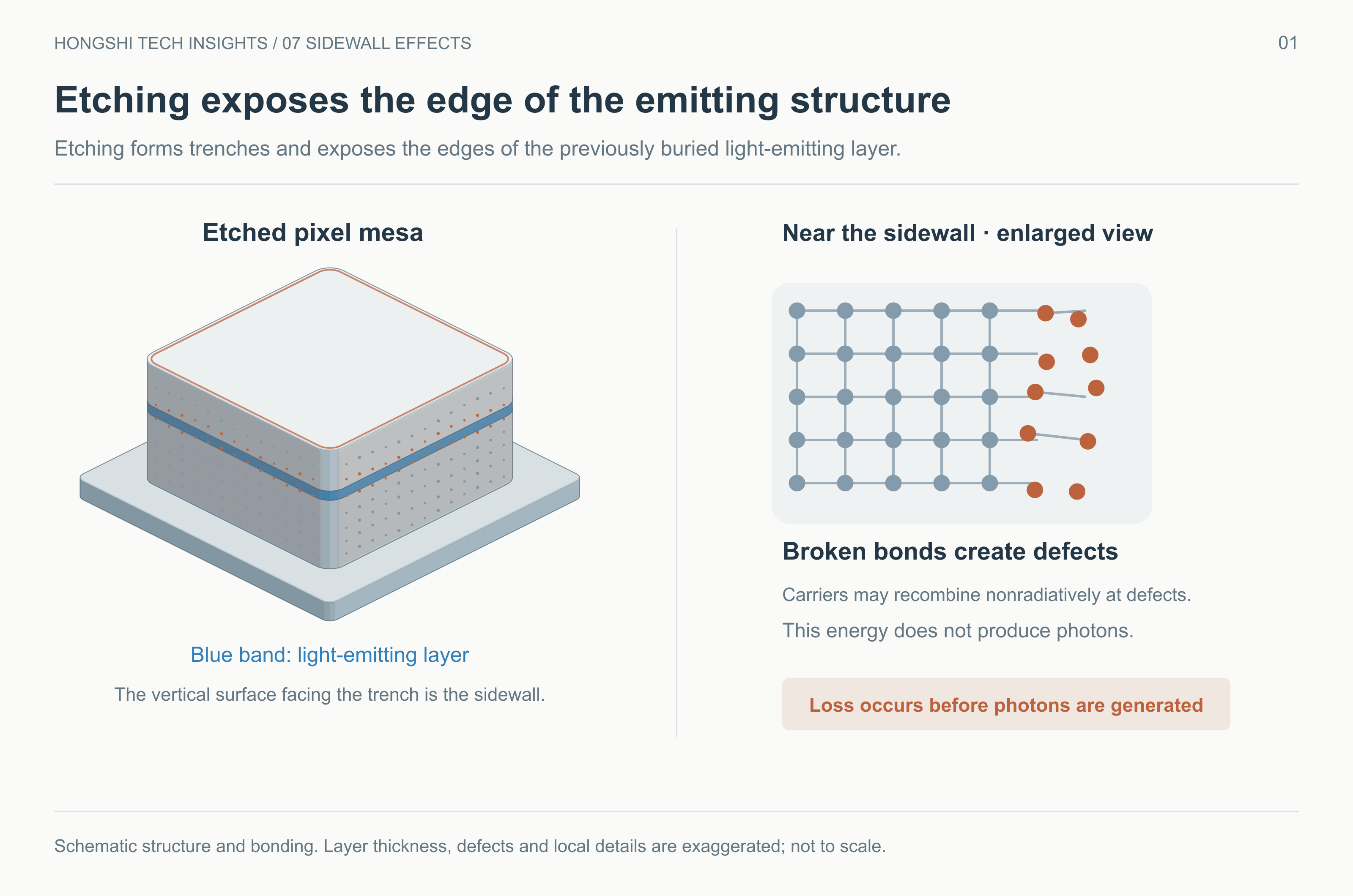
Consider a typical gallium nitride (GaN) based MicroLED with an etched mesa structure. Before pixel fabrication begins, the light-emitting structure has already been grown within the epitaxial wafer. Photolithography defines the individual pixel patterns, and etching removes GaN material from selected areas. The raised structures left behind are called mesas and form the pixels. Trenches separate the mesas, and the surfaces facing these trenches are the sidewalls. Material that was previously inside the wafer is now exposed as a new surface.
During etching, energetic particles bombard the sidewalls and break some of the bonds between atoms. This can cause defects such as lattice distortion, amorphous layers and dislocations. Cutting through the light-emitting layer also leaves many dangling bonds. As carriers encounter these defect sites, problems can arise, including nonradiative recombination, sidewall leakage current and heat generation.
With other conditions comparable, the more carriers recombine through these nonradiative pathways, the fewer remain available to produce light. The sidewall losses discussed here occur before photons are generated.
Why sidewalls matter more as pixels shrink
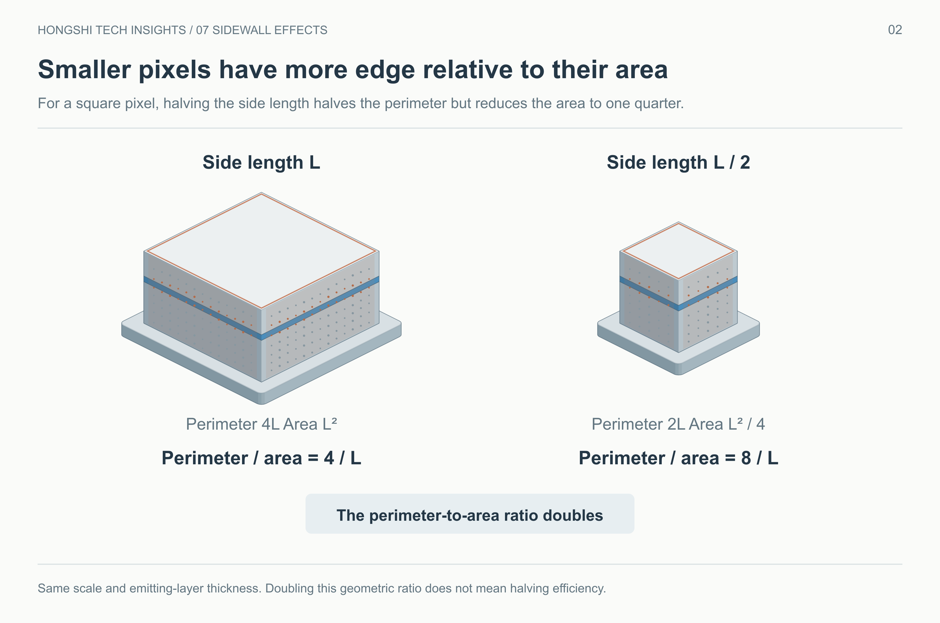
Imagine a square pixel. If its side length is halved, its perimeter also halves, but its area falls to one quarter of the original value. Its perimeter-to-area ratio therefore doubles.
For devices with the same light-emitting layer thickness, this means that the sidewalls become larger relative to the interior light-emitting region. Distances from the interior of the pixel to its edges also become shorter. With comparable sidewall quality and operating conditions, nonradiative recombination at the edges can therefore have a greater effect on the light emission of the whole pixel.
Doubling the perimeter-to-area ratio does not, however, mean that efficiency will be halved. The actual losses also depend on the number of defects, carrier transport and the condition of the sidewalls after treatment.
As pixels shrink, treating these edges becomes an important part of device fabrication.
Repair and passivation work together to reduce sidewall losses
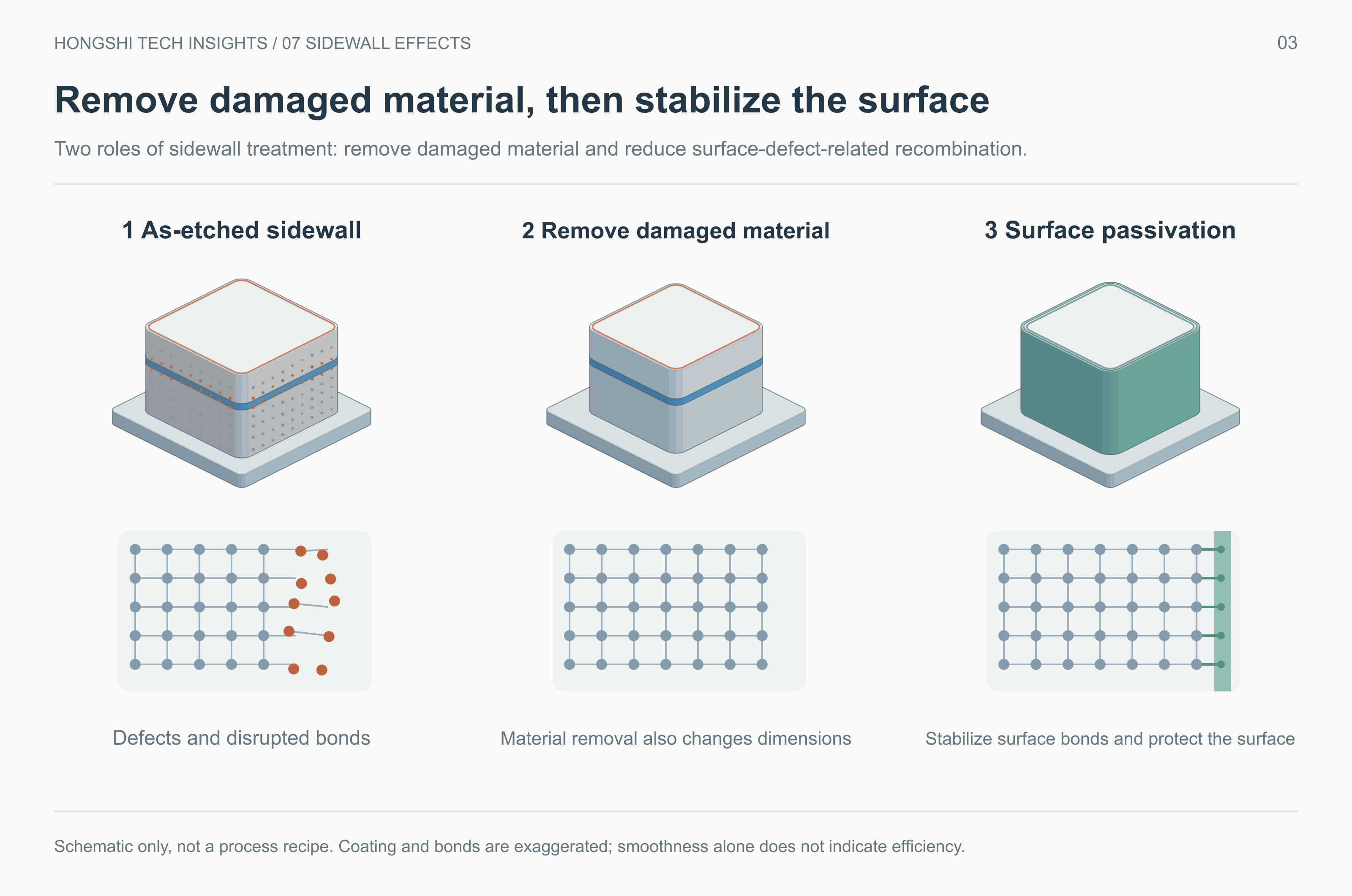
Reducing sidewall losses starts with limiting additional damage during etching. Once the sidewalls have been formed, further treatment is needed to address the damaged regions and improve the surface condition.
At Hongshi, we optimize our processes to control and repair sidewall damage, combining treatment of the damaged regions with surface passivation. To understand what each step does, we can follow the changes at the sidewall.
First, consider the damaged region.
Appropriate chemical treatment can remove some of the damaged material near the sidewall surface, reducing the extent of regions with a high concentration of defects. Here, “repair” can be achieved by removing damaged material; it does not mean restoring the original crystal lattice atom by atom.
Removing material also changes the pixel's dimensions and shape. Insufficient treatment may leave substantial damaged regions behind, while excessive treatment may cause the structure to deviate from the intended device design. With such small pixels, damage removal needs to be balanced against preserving the structure.
Next, consider the surface exposed by the treatment.
Appropriate surface passivation can saturate dangling bonds on the sidewall by forming stable chemical bonds, reducing nonradiative recombination associated with surface defects. The resulting coating can also protect the surface and reduce the influence of the surrounding environment. Passivation effectiveness depends on both the coating and the condition of its interface with the semiconductor.
Choosing a suitable treatment method is the starting point. How much damaged material to remove, which passivation conditions to use and how to control damage during subsequent processing all depend on the particular device. Even with the same type of treatment, different processing conditions and integration with preceding and subsequent steps can lead to different results.
These are the practical questions behind the sidewall process expertise we have built: applying our understanding of damage and surface condition to device fabrication so that sidewall treatment improves emission efficiency.
Improving EQE through sidewall process optimization
External quantum efficiency, or EQE, measures a device's ability to output photons. It is the ratio of the number of photons leaving the chip to the number of electrons injected. Reducing nonradiative recombination losses at the sidewalls helps more of the injected carriers contribute to the final light output.
For the devices and comparison conditions used in this sidewall process optimization, we achieved a 20% relative increase in MicroLED EQE.
This result gives sidewall treatment a concrete meaning: process control at the pixel edges can improve the device's ability to deliver photons.
From the outside, a pixel is just a tiny point of light. Efficient emission depends on both the light-emitting structure inside it and the edges left by fabrication. Our sidewall process optimization aims to minimize losses around those edges, allowing more of the injected carriers to contribute to light emission.